

The explosion of artificial intelligence (AI) has triggered an unprecedented demand for computing power. Major corporations like Amazon, MetaPlatforms, and Microsoft are pouring hundreds of billions of dollars into data centers and advanced chips developed by the American semiconductor giant Nvidia.
Meanwhile, China faces the risk of falling behind in this AI race, as US trade restrictions have cut off its access to core chip manufacturing technologies.
However, in this context, the Chinese technology giant Huawei has captured the full attention of investors and industry experts. Specifically, Huawei announced a completely new direction in semiconductor chip development that does not rely on advanced EUV lithography machines.
Technological breakthrough
Decades ago, Gordon Moore, co-founder of Intel, predicted that advances in semiconductor manufacturing processes would allow the number of transistors on an integrated circuit to roughly double every two years.
This observation, known as Moore's Law, held true for decades as smaller transistors, packed more densely, increased efficiency and reduced power consumption.
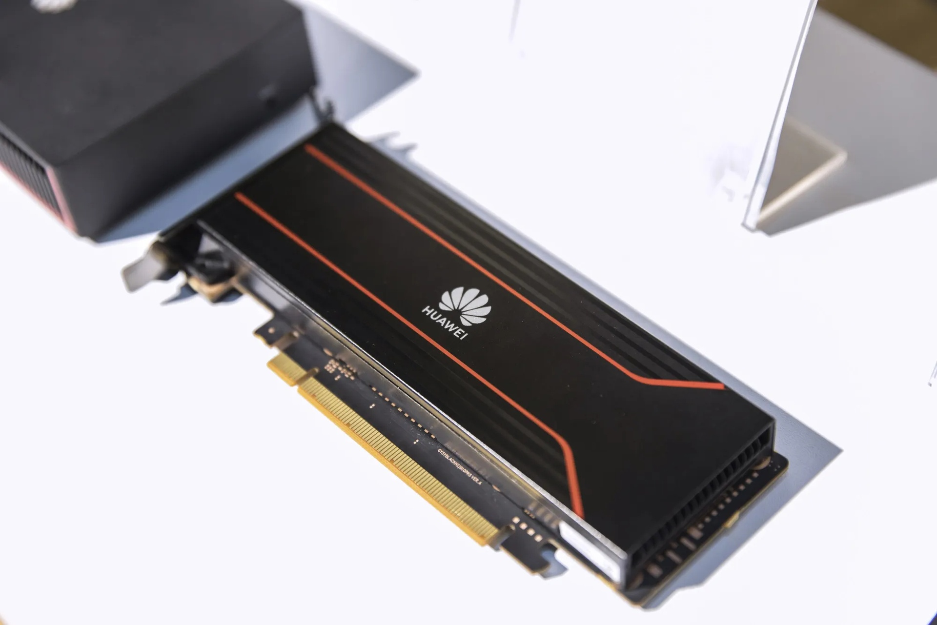 |
Huawei announces an unprecedented approach to semiconductor chip development. Photo: Bloomberg. |
However, Huawei's proposed Tau Ratio Law seeks to break away from that model. Instead of trying to shrink transistors to the extreme, this law focuses on improving performance by shortening the distance data has to travel inside the processor.
Based on this principle, Huawei simultaneously announced LogicFolding architecture, a technology capable of reducing resistance and capacitance during signal transmission, thereby increasing transistor density without the need for improvements in lithography tools.
This idea isn't actually new. Leading chip designers like Taiwan's TSMC have long used advanced stacking technologies. However, Huawei's solution proposes a bolder and more radical restructuring right from the core structure of the chip.
This approach will undoubtedly face significant technical challenges, including manufacturing complexity, heat dissipation, and power supply issues. Whether this technology can be implemented economically and on a large scale remains to be seen.
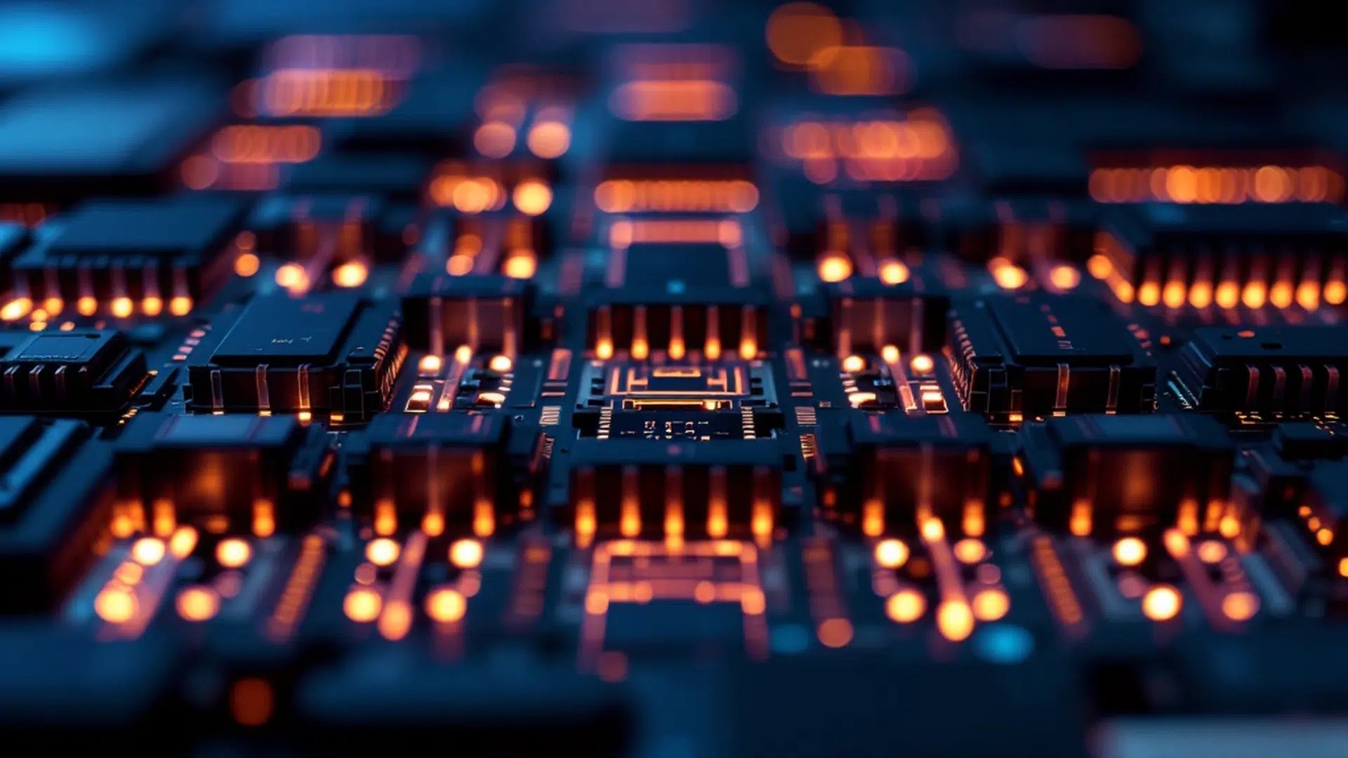 |
Huawei's Tau Ratio Law proposes a bolder and more radical restructuring, starting from the core structure of the chip. Photo: Futurum Group. |
Nevertheless, Huawei has outlined an ambitious roadmap for LogicFolding and announced plans to launch its first chips using this technology in smartphones this year. Even bolder, the company aims to achieve transistor density equivalent to the 1.4 nm process by 2031.
This is among the most advanced technologies in the world today, on par with the roadmap that TSMC and Samsung are pursuing with their massive investments in the latest generation of EUV machines.
The key point in Huawei's statement is when Ms. He asserted that improving lithography technology would "no longer be essential" in the company's new direction. This is a direct signal aimed at the biggest bottleneck in China's semiconductor industry.
The significance of survival
Under US sanctions, Chinese companies are now prohibited from purchasing EUV machines from the Dutch monopoly manufacturer ASML. In theory, they cannot produce chips at 3 nm or less using traditional methods.
With LogicFolding, Huawei appears to be seeking to bypass this very hurdle. If successful, this breakthrough would help the Chinese giant circumvent trade sanctions by improving chip performance through innovative design and packaging, rather than relying on restricted machine technologies.
Furthermore, this advancement could help Huawei narrow the technological gap with major rivals like TSMC. With LogicFolding, Huawei aims to produce semiconductors with performance equivalent to 1.4 nm process chips by 2031.
Although this target still puts Huawei a few years behind its rivals (TSMC aims to achieve similar progress by 2028), it would represent a significantly narrower gap compared to the multi-generational lag that Huawei and SMIC currently face.
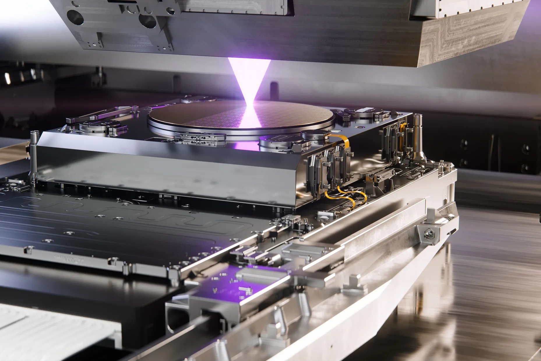 |
With LogicFolding, Huawei appears to be trying to bypass the barrier of not being able to access EUV technology. Photo: ASML. |
However, the gap between the claims and the reality of mass production remains a major question. Adding more layers to a stacked chip structure significantly increases the complexity of the manufacturing process, while also increasing the error rate, which risks reducing the yield of commercially viable chips.
In addition, the stacking method also creates significant thermal challenges. Densely stacked chips tend to retain more heat and require more advanced cooling systems.
Meanwhile, one of the biggest advantages of traditional flat chip architecture is the maximization of surface area for heat dissipation.
However, this isn't the first time Huawei has surprised people with its chip manufacturing process. In 2023, the company launched the Mate 60 Pro with the Kirin 9000S chip, manufactured using a 7nm process, surprising many Western experts who believed China couldn't achieve this under sanctions.
Source: https://znews.vn/vi-sao-huawei-khien-gioi-cong-nghe-day-song-post1654890.html
![[Image] Nearly 125,000 Hanoi students completed the Literature exam for the 10th grade entrance exam.](https://vphoto.vietnam.vn/thumb/1200x675/vietnam/resource/IMAGE/2026/05/30/1780117233041_ndo_br_thiet-ke-chua-co-ten-2-png.webp)






























































































Comment (0)