

 |
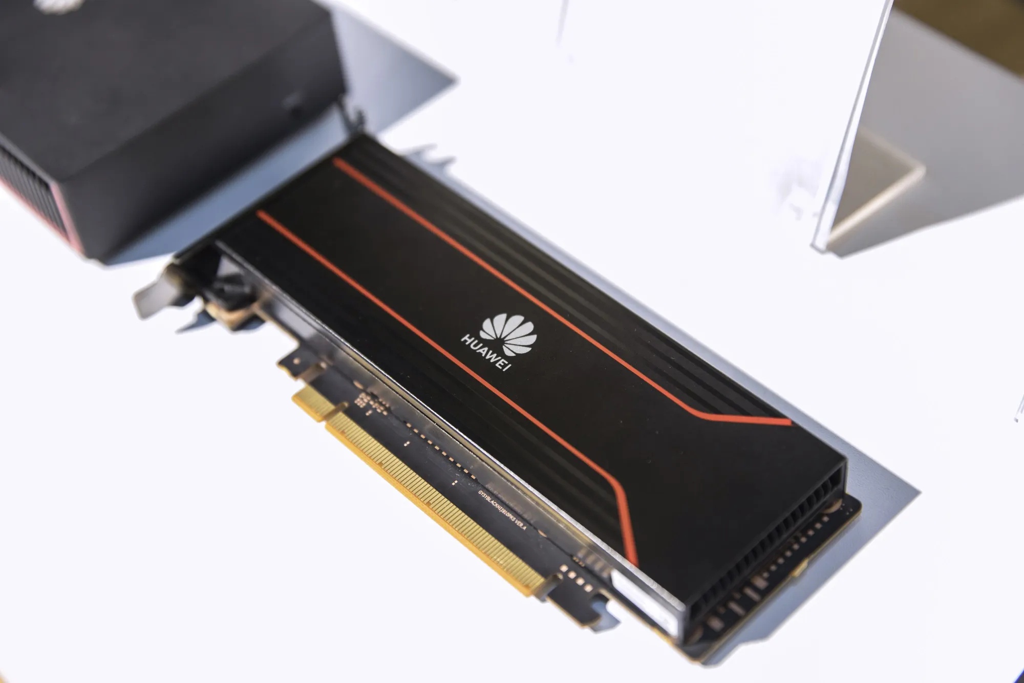
Huawei announces new direction for chip development and production. Photo: Bloomberg . |
Huawei has just announced a completely new direction in semiconductor chip development, moving away from advanced EUV lithography machines.
At a press conference on May 25, He Tingbo, Chair of the Science Committee and head of Huawei's semiconductor division, presented the Tau Ratio Law (τ), a new principle that Huawei describes as guiding "the evolution of both semiconductors and electronic systems."
Based on this principle, Huawei simultaneously announced LogicFolding architecture, a technology capable of reducing resistance and capacitance during signal transmission, thereby increasing transistor density without improving the lithography tool. The company aims to achieve transistor density equivalent to the 1.4 nm process by 2031.
This is among the most advanced technologies in the world today, on par with the roadmap that TSMC and Samsung are pursuing with their massive investments in the latest generation of EUV machines.
The key point in Huawei's statement is when Ms. He asserted that improving lithography technology would "no longer be essential" in the company's new direction. This is a direct signal aimed at the biggest bottleneck in China's semiconductor industry.
Under US sanctions, Chinese companies are now prohibited from purchasing EUV machines from the Dutch monopoly manufacturer ASML. In theory, they cannot produce chips at 3 nm or less using traditional methods. If the LogicFolding architecture works as advertised, Huawei is seeking to circumvent this very barrier.
This isn't the first time Huawei has surprised people with its chip manufacturing process. In 2023, the company launched the Mate 60 Pro with the Kirin 9000S chip, manufactured using a 7nm process, surprising many Western experts who believed China couldn't achieve this under sanctions.
However, the gap between the stated specifications and the reality of mass production remains a major question. Achieving a transistor density equivalent to 1.4 nm in theory is one thing. Mass production with an acceptable error rate is an entirely different problem. This is a point that even TSMC and Samsung have taken years to resolve with each new generation of technology.
Nevertheless, Huawei's statement is a noteworthy signal. It shows that China is proactively seeking its own path in semiconductor development instead of waiting for the embargo to be lifted.
Source: https://znews.vn/huawei-thach-thuc-linh-vuc-chip-post1654119.html
![[Photo] The courage of new recruits of Brigade 144 on the training ground.](https://vphoto.vietnam.vn/thumb/1200x675/vietnam/resource/IMAGE/2026/05/27/1779881651341_anh-man-hinh-2026-05-27-luc-18-32-52.png)



![[Photo] General Secretary and President To Lam and his wife begin their official visit to Thailand.](https://vphoto.vietnam.vn/thumb/1200x675/vietnam/resource/IMAGE/2026/05/27/1779881249412_anh-man-hinh-2026-05-27-luc-18-10-51.png)
















![[Photo] The heat at the fireworks display site on the opening night of the Da Nang International Fireworks Festival 2026](https://vphoto.vietnam.vn/thumb/1200x675/vietnam/resource/IMAGE/2026/05/27/1779889741485_ndo_br_z7872039145157-fecaba5112f39e8352544099d7ef4738-5140-jpg.webp)

































![[Photo] The courage of new recruits of Brigade 144 on the training ground.](https://vphoto.vietnam.vn/thumb/402x226/vietnam/resource/IMAGE/2026/05/27/1779881651341_anh-man-hinh-2026-05-27-luc-18-32-52.png)




























Comment (0)