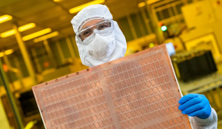
According to Engadget , Intel says its new glass substrate will be more durable and efficient than existing organic materials. The glass will also allow the company to place multiple chiplets and other components side-by-side. This could present challenges for the company regarding bending and instability compared to existing silicon packages using organic materials.

Intel boasts a breakthrough in substrate manufacturing technology.
Intel stated in a press release that: "Glass substrates can withstand higher temperatures, reduce pattern distortion by less than 50%, and have extremely low flatness to improve focal depth for lithographic printing, while providing the dimensional stability needed for extremely tight interlayer bonding."
With these capabilities, the company claims that the glass substrate will also help increase connection density by up to 10 times, as well as enable the creation of "ultra-large packages with high assembly productivity".
Intel is reportedly investing heavily in the design of future chips. Two years ago, the company announced its "gate-all-around" transistor design, RibbonFET, as well as PowerVia, which allows it to route power to the back of the chip's semiconductor wafer. At the same time, Intel also announced it would build chips for Qualcomm and Amazon's AWS service.
Intel added that we will first see chips using glass dies in high-performance areas, such as AI (artificial intelligence), graphics, and data centers. This glass breakthrough is another sign that Intel is also ramping up its advanced packaging capabilities at its US foundries.
Source link


![[Photo] Prime Minister Pham Minh Chinh receives the Chinese Ambassador to Vietnam](https://vphoto.vietnam.vn/thumb/1200x675/vietnam/resource/IMAGE/2026/04/05/1775397481797_ndo_br_dsc-5512-jpg.webp)


Comment (0)